Current electron diffraction simulation software primarily supports single-phase simulations. However, for advanced analysis involving twinning, multiple phases with fixed orientations, and comparing diffraction patterns from different phases, existing functionalities may be insufficient. Key tasks in electron diffraction analysis include determining the zone axis, indexing diffraction patterns for phase identification, and orienting crystal grains. To enhance structural interpretation and modeling, a projected atomic potential (difference) map can aid in interpreting high-resolution electron microscopy (HREM) images. This capability is integrated as an extension in ESPOT. Therefore, we have developed SAED, currently in its 6th version, to address these needs comprehensively. Simulating electron diffraction patterns for twins and multiple coexisting phases involves calculating patterns from multiple structures within a single frame. SAED is designed to sequentially calculate patterns from multiple structures, making it easy to adjust and simulate patterns from twins and multiple coexisting structures with fixed orientations. · A window frame with a panel displays the simulated pattern or matches a preloaded experimental diffraction pattern. · Input parameters for calculations can be initialized using an operational panel and several dialog windows. · Structure data files can be easily prepared using a computer assistant template. · Multiple phases can be loaded and calculated simultaneously to simulate diffraction patterns for twins, coexisting phases with fixed orientations, and for comparing similar patterns from different phases. · Experimental patterns can be aligned, resized, and rotated. |
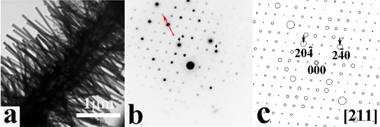
TEM images of the hierarchical structure (a). Experimental EDPs of the Cu2S nanowires (b), arrows show the nanowire growth direction and corresponding simulated patterns of monoclinic Cu2S crystal structure (c).